
iPhone 18 Pro Max Charging Circuit Schematic – KiCad Documentation
Understanding modern smartphone charging architecture is an important part of advanced smartphone hardware troubleshooting and repair.
As part of my smartphone hardware reverse-engineering and training activities, I have created a conceptual iPhone 18 Pro Max Charging Circuit Schematic using KiCad.
This documentation brings together the major charging-related components, power paths, battery connections, and associated circuit sections in a single schematic for easier understanding and technical training.
About This Project
The objective of this project is to organize and represent the iPhone 18 Pro Max charging section in a structured schematic format. Instead of referring to individual circuit blocks separately, this documentation provides a conceptual overview of the major charging-related components and their connections.
The schematic was designed using KiCad EDA 10.0.4, with a focus on readability, circuit identification, and educational understanding.
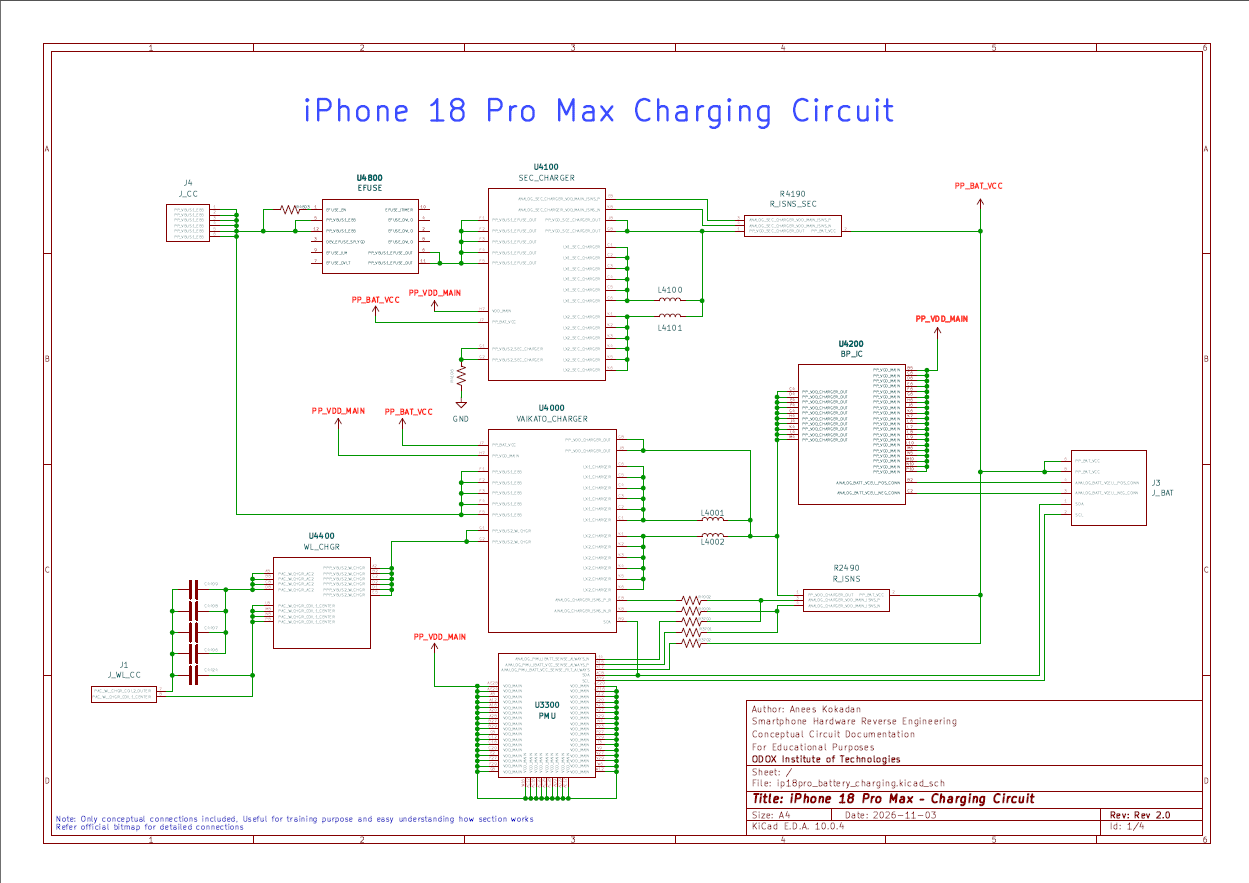
Figure 1: iPhone 18 Pro Max Charging Circuit – Rev 2.0
Major Circuit Sections
The schematic covers several important charging and power management components. The following sections are identified in the conceptual circuit documentation.
1. USB-C Input Section
The J4 USB-C connector section includes the PP_VBUS1_E85 input connections, representing the wired charging input path.
2. eFuse – U4800
The EFUSE section includes control and protection-related signals such as EFUSE_EN, EFUSE_OVLO, EFUSE_ILM, and the PP_VBUS1_EFUSE_OUT power path.
3. Secondary Charger – U4100
The SEC_CHARGER block includes charging-related power connections, LX1/LX2 switching nodes, and battery current-sensing connections.
4. Main Charger – U4000
The VAIKATO_CHARGER block is represented with its associated input, output, switching, and current-sensing connections.
5. Wireless Charging – U4400
The WL_CHGR section includes wireless charging-related connections, including coil interfaces and associated capacitor connections.
6. Battery Interface – J3
The battery connector section includes battery voltage sensing connections, battery supply, SDA, and SCL signals.
7. Battery Power Interface – U4200
The BP_IC block is represented with connections to PP_VDD_MAIN and battery-related sensing and interface signals.
8. Power Management – U3300
The PMU section illustrates the VDD_MAIN power connections and associated power-management interfaces in the conceptual schematic.
Important Power Lines and Signals
Some of the important power nets and signals identified in this schematic include:
- PP_VBUS1_E85 – USB-C input power net.
- PP_VBUS1_EFUSE_OUT – eFuse output power net.
- PP_BAT_VCC – Battery supply connection.
- PP_VDD_MAIN – Main system power rail.
- PP_VDD_CHARGER_OUT – Charger output power net.
- LX1 / LX2 – Switching-node connections.
- ANALOG_CHARGER_ISNS – Charger current-sensing signals.
- ANALOG_BATT_VCELL – Battery voltage-sensing connections.
Why I Created This Schematic
While teaching smartphone hardware technology, I believe understanding circuit architecture is just as important as practical troubleshooting.
Creating conceptual schematics helps students and technicians understand how different circuit sections are represented, identify important components, follow power connections, and develop their circuit-analysis skills.
This project is also part of my continuous effort to develop structured technical learning resources for smartphone hardware reverse engineering.
Download the Schematic PDF
iPhone 18 Pro Max – Charging Circuit
Get the Rev 2.0 conceptual schematic documentation in PDF format.
View PDF Download Schematic