Here is a brief description of my experiment about smartphone charging logic signal analysis, and this article may be helpful for smartphone technicians during troubleshooting charging related faults in smartphone.
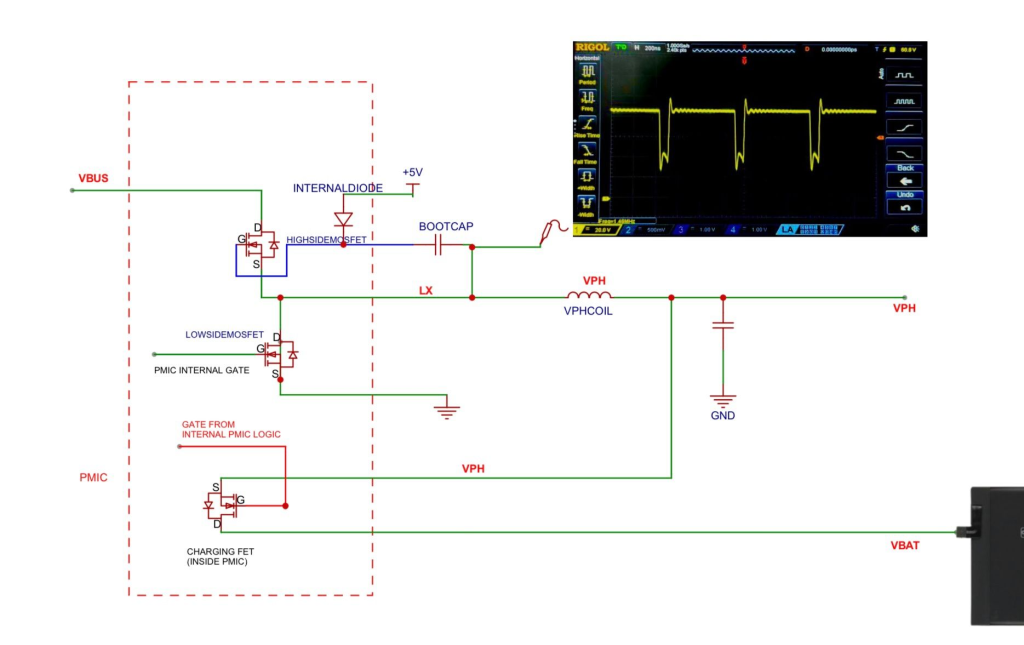
Charging section circuit flow:
1. Vbus connected
2. Low side MOSFET becomes ON ( high side MOSFET OFF)
3. Lx pin 0v
4. Boot cap charges 5v via internal diode
5. High side MOSFET becomes ON, (low side MOSFET OFF )
6. Lx voltage transition 0 to 4.2v, boot pin voltage transition 5 to 9.2 (capacitor already charged 5v + 4.2v )
7. Low side MOSFET becomes ON, LX voltage = 0v, Vph coil releases current to vph section and battery
8. High side MOSFET ON and this process continues…
if we use fast charger with 9v etc.. the speed of LX switching increases ie; Lx switching frequency increases, but value of Vph remains the same as 4.2v, and current flow in the Vph side increases, now the battery will charge more faster than normal charging
Charging flow :
Vbus –> high side MOSFET –> LX –> Vph coil ( here ampere increases due to the combined working of high side mosfet, low side mosfet, boot cap and buck coil) –> Vph path –> PMIC internal battery charging MOSFET–> battery 🔋
If fast charger is used,
Lx wave form amplitude increases and duty cycle decreases to maintain correct 4.2 output voltage; frequency of LX signal increases
According to my experiment, I got a frequency of 750KHz on LX pin when I connected normal charging, and I got 2.5MHz on LX pin when I used fast charger.
When we use fast charger amplitude of the Lx wave form also increases to 9v ( depends upon the input vbus voltage)
The charging MOSFET at the output side is responsible for charging current limiting and auto cutoff the circuit when battery becomes full, current sensing etc ..